2009 VLSI (NCTU, S.Chung, eSiGe on extension)
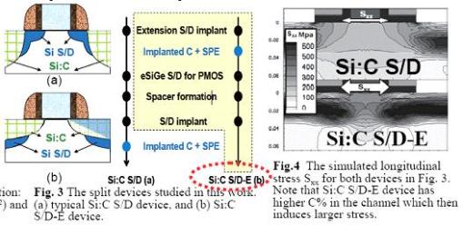
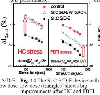
Chung, S.S.; Hsieh, E.R.; Liu, P.W.; Chiang, W.T.; Tsai, S.H.; Tsai, T.L.; Huang, R.M.; Tsai, C.H.; Teng, W.Y.; Li, C.I.; Kuo, T.F.; Wang, Y.R.; Yang, C.L.; Tsai, C.T.; Ma, G.H.; Chien, S.C.; Sun, S.W., “Design of high-performance and highly reliable nMOSFETs with embedded Si:C S/D extension stressor(Si:C S/D-E),” VLSI Technology, 2009 Symposium on , vol., no., pp.158-159, 16-18 June 2009
Abstract: A Novel strained nMOSFET with embedded Si:C in S/D extension stressor (Si:C S/D-E) was presented. Comparing to the bulk device, it revealed good drive current ION (+27%), high ID,sat current (+67%), enhanced channel mobility (+105%), at a lower effective substitutional carbon concentration (C%=1.1%), using the poly-gate 40 nm-node Si:C/eSiGe S/D CMOS technology. Moreover, PBTI effect was first observed in this device as a result of carbon impurity out-diffusion, which is of critically important for the design trade-off between performance and reliability.
URL: http://ieeexplore.ieee.org/stamp/stamp.jsp?arnumber=5200671&isnumber=5200578
2009 VLSI TSA
Liu, P.W.; Kuo, T.F.; Li, C.I.; Wang, Y.R.; Huang, R.M.; Tsai, C.H.; Tsai, C.T.; Ma, G.H., “Dopant and thermal interaction on SPE formed SiC for NMOS performance enhancement,” VLSI Technology, Systems, and Applications, 2009. VLSI-TSA ‘09. International Symposium on , vol., no., pp.24-25, 27-29 April 2009
Abstract: The dopant and thermal interaction on solid phase epitaxy (SPE) formed SiC has been investigated. We have studied the impact on substitutional carbon concentration ([C]sub) from various thermal steps including low temperature anneal, SiGe epitaxy thermal budget, RTP, and laser anneal (LSA). Regarding the integration scheme for implementing embedded SiC (eSiC) S/D on NMOS performance enhancement, both post-LDD and post-S/D schemes were studied. The higher [C]sub in post-LDD scheme was observed and the S/D dopants were found to enhance the carbon precipitation into interstitial with conventional RTP/LSA activation thermal processes. The phosphorous implant is also found to degrade [C]sub in comparison to As implant. The higher [C]sub and proximity to channel of formed eSiC in post-LDD scheme are beneficial to device performance. The fabricated eSiC S/D NMOS shows 31% mobility improvement and 7% current enhancement.
URL: http://ieeexplore.ieee.org/stamp/stamp.jsp?arnumber=5159275&isnumber=5159260
2008 IEDM
Yang, B.; Takalkar, R.; Ren, Z.; Black, L.; Dube, A.; Weijtmans, J.W.; Li, J.; Johnson, J.B.; Faltermeier, J.; Madan, A.; Zhu, Z.; Turansky, A.; Xia, G.; Chakravarti, A.; Pal, R.; Chan, K.; Reznicek, A.; Adam, T.N.; de Souza, J.P.; Harley, E.C.T.; Greene, B.; Gehring, A.; Cai, M.; Aime, D.; Sun, S.; Meer, H.; Holt, J.; Theodore, D.; Zollner, S.; Grudowski, P.; Sadana, D.; Park, D.-G.; Mocuta, D.; Schepis, D.; Maciejewski, E.; Luning, S.; Pellerin, J.; Leobandung, E., “High-performance nMOSFET with in-situ phosphorus-doped embedded Si:C (ISPD eSi:C) source-drain stressor,” Electron Devices Meeting, 2008. IEDM 2008. IEEE International , vol., no., pp.1-4, 15-17 Dec. 2008
Abstract: For the first time, embedded Si:C (eSi:C) was demonstrated to be a superior nMOSFET stressor compared to SMT or tensile liner (TL) stressors. eSi:C nMOSFET showed higher channel mobility and drive current over our best poly-gate 45 nm-node nMOSFET with SMT and tensile liner stressors. In addition, eSi:C showed better scalability than SMT plus tensile liner stressors from 380 nm to 190 nm poly-pitches.
URL: http://ieeexplore.ieee.org/stamp/stamp.jsp?arnumber=4796611&isnumber=4796592
2008 EDL
Verheyen, P.; Machkaoutsan, V.; Bauer, M.; Weeks, D.; Kerner, C.; Clemente, F.; Bender, H.; Shamiryan, D.; Loo, R.; Hoffmann, T.; Absil, P.; Biesemans, S.; Thomas, S.G., “Strain Enhanced nMOS Using In Situ Doped Embedded $hbox{Si}_{1 – x}hbox{C}_{x}$ S/D Stressors With up to 1.5% Substitutional Carbon Content Grown Using a Novel Deposition Process,” Electron Device Letters, IEEE , vol.29, no.11, pp.1206-1208, Nov. 2008
Abstract: This letter reports on the implementation of high carbon content and high phosphorous content Si1-xCx layers in the source and drain regions of n-type MOSFET in a 65-nm-node integration scheme. The layers were grown using a novel epitaxial process. It is shown that by implementing stressors with x ap 0.01, nMOSFET device performance is enhanced by up to 10%, driving 880 muA/mum at 1-V V DD. It is also demonstrated that the successful implementation of Si1-xCx relies on the careful choice of integration and epitaxial layer parameters. There is a clear impact of the postepitaxial implantation and thermal treatment on the retained substitutional C content ([C sub]). Furthermore, adding a Si capping layer on top of the Si1 -xCx, greatly improves upon the stressors’ stability during the downstream processing and the silicide sheet resistance.
URL: http://ieeexplore.ieee.org/stamp/stamp.jsp?arnumber=4655506&isnumber=4655490
2008 VLSI
Zhibin Ren; Pei, G.; Li, J.; Yang, B.F.; Takalkar, R.; Chan, K.; Xia, G.; Zhu, Z.; Madan, A.; Pinto, T.; Adam, T.; Miller, J.; Dube, A.; Black, L.; Weijtmans, J.W.; Yang, B.; Harley, E.; Chakravarti, A.; Kanarsky, T.; Pal, R.; Lauer, I.; Park, D.-G.; Sadana, D., “On implementation of embedded phosphorus-doped SiC stressors in SOI nMOSFETs,” VLSI Technology, 2008 Symposium on , vol., no., pp.172-173, 17-19 June 2008
Abstract: We report a successful implementation of epitaxially grown Phosphorus-doped (P-doped) embedded SiC stressors into SOI nMOSFETs. We identify a process integration scheme that best preserves the SiC strain and minimizes parasitic resistance. At a substitutional C concentration (Csub) of ~1.0%, high performance nFETs with SiC stressors demonstrate ~9% enhanced Ieff and ~15% improved Idlin against the well calibrated control devices. It is found that the tensile liner technique provides further performance improvement for nFETs with SiC stressors, whereas the stress memory technique (SMT) does not provide performance gain in a laser annealing process that is used to preserve SiC strain. The material quality of the SiC stressors strongly affects strain transfer.
URL: http://ieeexplore.ieee.org/stamp/stamp.jsp?arnumber=4588607&isnumber=4588540
2005 IEDM
Kah-Wee Ang; King-Jien Chui; Bliznetsov, V.; Yihua Wang; Lai Yin Wong; Chih-Hang Tung; Balasubramanian, N.; Ming-Fu Li; Ganesh Samudra; Yee-Chia Yeo, “Thin body silicon-on-insulator N-MOSFET with silicon-carbon source/drain regions for performance enhancement,” Electron Devices Meeting, 2005. IEDM Technical Digest. IEEE International , vol., no., pp.497-500, 5-5 Dec. 2005
Abstract: We report a novel strained n-channel transistor structure featuring silicon-carbon (SiC) source and drain (S/D) regions formed on thin body SOI substrate. The SiC material is pseudomorphically grown by selective epitaxy and the carbon mole fraction incorporated is 1%. Lattice mismatch between SiC and Si results in uniaxial tensile strain in the Si channel region which contributes favorably to electron mobility enhancement. Drive current IDsat enhancement of 25% was observed for 90 nm gate length LG transistors, and IDsat enhancement of up to 35% was observed at LG of 70 nm. In addition, drive current enhancement shows dependence on device width and channel orientation. All transistors were formed on (001) SOI substrates. The largest IDsat enhancement is observed for transistors with the [010] channel orientation
URL: http://ieeexplore.ieee.org/stamp/stamp.jsp?arnumber=1609390&isnumber=33791
2004 IEDM
Kah Wee Ang; King Jien Chui; Bliznetsov, V.; Anyan Du; Balasubramanian, N.; Ming Fu Li; Ganesh Samudra; Yee-Chia Yeo, “Enhanced performance in 50 nm N-MOSFETs with silicon-carbon source/drain regions,” Electron Devices Meeting, 2004. IEDM Technical Digest. IEEE International , vol., no., pp. 1069-1071, 13-15 Dec. 2004
Abstract: This paper reports a novel strained N-channel transistor structure with sub-100 nm gate lengths. The strained N-MOSFET features silicon-carbon (SiC) source and drain (S/D) regions formed by a Si recess etch and a selective epitaxy of SiC in the S/D regions. The carbon mole fraction incorporated is 1.3%. Lattice mismatch of 0.65% between SiC and Si results in horizontal tensile strain and vertical compressive strain in the Si channel region, both contributing to substantial electron mobility enhancement. The conduction band offset Ec between the SiC source and the strained-Si channel also contributes to increased electron injection velocity from the source. Implementation of the SiC stressors provides significant drive current IDS enhancement in the N-MOSFETs. IDS enhancement of 50% was observed for a gate length of 50 nm.
URL: http://ieeexplore.ieee.org/stamp/stamp.jsp?arnumber=1419383&isnumber=30682


